
8 Channel 12bit 250 MS/s Digitizer
VX1720
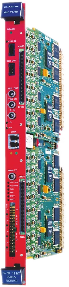
The VX1720 is a 1-unit wide VME64X 6U module housing a 8 Channel 12 bit 250 MS/s Flash ADC Waveform Digitizer and featuring 2 Vpp single ended input dynamics.
The DC offset adjustment (range ±1 V) by programmable 16bit DACs (one for each channel) on single ended input versions allows a right sampling of a bipolar (Vin = ±1 V) up to a full positive (Vin = 0 ÷ +2 V) or negative (Vin = 0 ÷ -2 V) analog input swing without losing dynamic resolution.
The module features front panel Clock Input and Output as well as a PLL for clock synthesis from internal/external references. The data stream is continuously written in a circular memory buffer. When the trigger occurs, the FPGA writes further N samples for the post trigger and freezes the buffer that can be read either by VMEbus or Optical Link. The acquisition can continue without dead time in a new buffer.
Each channel has a SRAM Multi-Event Buffer divisible into 1 ÷ 1024 buffers of programmable size. Two sizes of the channel digital memory are available by ordering options: 1.25 MS/ch (mod. VX1720E) and 10 MS/ch (mod. VX1720G). “Zero suppression” and “data reduction” algorithms allow substantial savings in data amount readout and processing, rejecting samples smaller than programmable threshold. VX1720 supports multi-board synchronization allowing all ADCs to be synchronized to a common clock source and ensuring Trigger time stamp alignment. Once synchronized, all data will be aligned and coherent across multiple VX1720 boards.
The trigger signal can be provided externally via the front panel Trigger Input as well as via the software, but it can also be generated internally thanks to threshold self-trigger capability. The trigger from one board can be propagated to the other boards through the front panel Trigger Output.
An Analog Output is available with four operating modes supported:
-
Waveform Generator: 1 Vpp ramp generator
-
Majority: output signal is proportional to the number of ch. under/over threshold (1 step = 125 mV)
-
Buffer Occupancy: output signal is proportional to the Multi Event Buffer Occupancy: 1 buffer ~ 1 mV
-
Voltage level: output signal is a programmable voltage level
VX1720 houses VME (VME64X compliant) and Optical Link interfaces. The VME interface allows data transfers of 60 MB/s (MBLT64), 100 MB/s (2eVME), 160 MB/s (2eSST). The Optical Link supports transfer rate of 80 MB/s and offers Daisy chain capability. Therefore, it is possible to connect up to 8/32 ADC modules to a single Optical Link controller (Mod. A2818/A3818).
Software available (Windows and Linux):
CAEN provides drivers for all the different types of physical communication channels, a set of C and LabView libraries (CAENComm and CAENDigitizer), demo applications and utilities:
-
CAENSCOPE: fully graphical program that implements a simple oscilloscope.
-
CAENUpgrader: tool that allows the user to update the firmware of the digitizers, change the PLL settings, load, when requested, the license for the pay firmware and other utilities.
-
CAEN WaveDump: software console application that can be used to configure and readout event data from any model of the CAEN digitizer family and save the data into a memory buffer allocated for this purpose.
CAEN provides also for this model Digital Pulse Processing firmware for Physics Applications. This feature allows to perform on-line processing on detector signal directly digitized:
-
DPP-PSD Digital Pulse Processing for Pulse Shape Discrimination
x720(*) and x751 digitizers running DPP-PSD firmware accept signals directly from the detector and implement a digital replacement of dual gate QDC, discriminator and gate generator.
(*) DPP-CI firmware and DPP-CI Control Software are no longer supported. To perform Charge Integration please refer to the DPP-PSD firmware and software
The VX1720 fits in the single-slot CAEN VME64X u-crate, which allows you to convert the VME digitizer into a desktop board for lab tests.
Features
-
12 bit 250 MS/s ADC
-
FPGA for real time Digital Pulse Processing:
-
Zero Suppression (Waveform Recording Firmware)
-
8 channels
-
2 Vpp input range (single ended)
-
16-bit programmable DC offset adjustment: ±1 V
-
Trigger Time stamps
-
Memory buffer: 1.25 or 10 MS/ch, up to 1024 events
-
Programmable event size and pre-post trigger adjustment
-
Analog Sum/Majority and digital over/under threshold flags for Global Trigger logic
-
Front panel clock In/Out available for multiboard synchronisation (direct feed through or PLL based synthesis)
-
16 programmable LVDS I/Os
-
VME64X compliant interface
-
Optical Link interface (CAEN proprietary protocol)
-
A2818 (PCI) / A3818 (PCIe) Controller available for handling up to 8/32 modules Daisy chained via Optical Link
-
Firmware upgradeable via VME/Optical Link
-
Libraries, Demos (C and LabView) and Software tools for Windows and Linux
Accessories
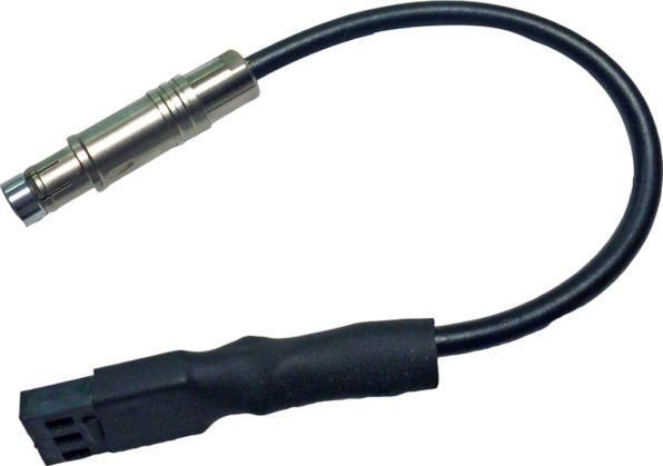
A318
Adapter for Clock signal FISCHER S101A004 male to 3-pin AMPMODU IV female – 10 cm
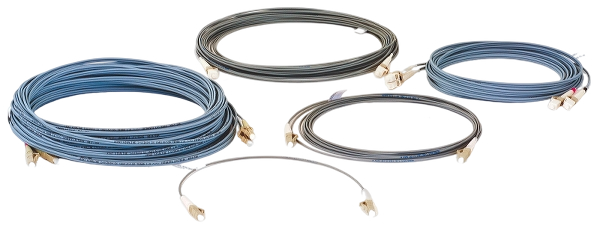
AI2700
Optical Fiber Series
A317
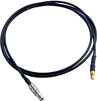
Cable assembly for Clock distribution 3-pin AMPMODU IV female terminations – 18 cm / 25cm
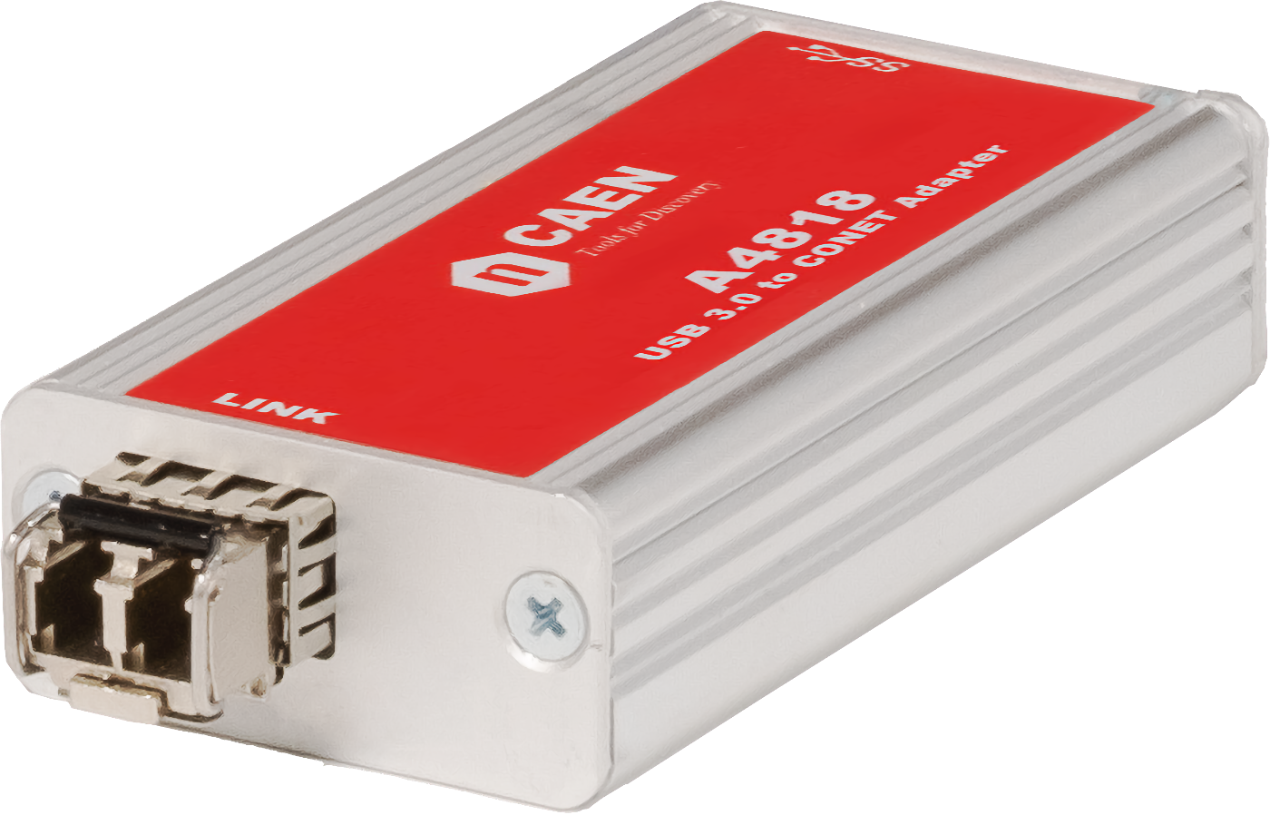
A4818
USB 3.0 to CONET2 Adapter
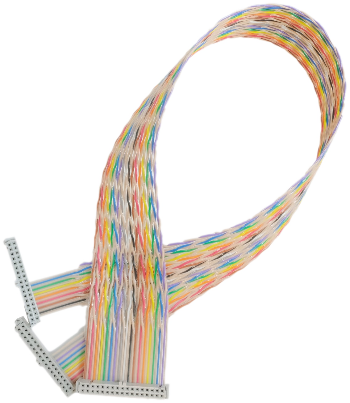
A953
Cable assembly 2.54mm 34 pin female to two 2.54mm 34 pin female – 50 cm
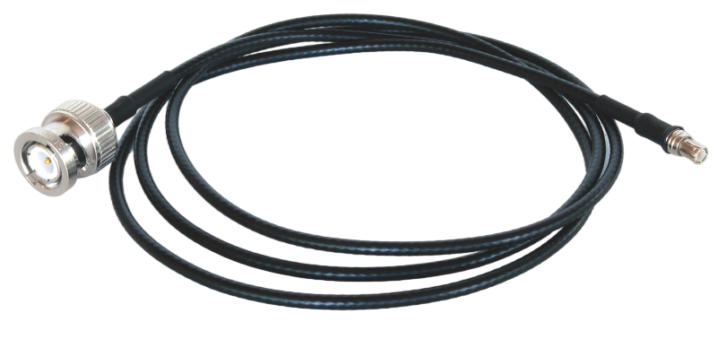
A659
Cable assembly BNC male to MCX male – 1 m
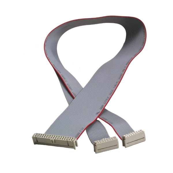
A954
Cable assembly 2.54mm 34 pin female to two 2.54mm 16 pin female - 50 cm
A952
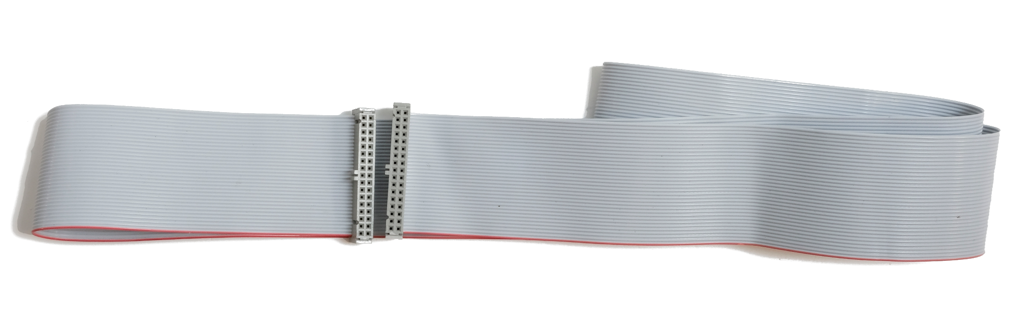
Cable assembly 2.54mm 34 pin female to 2.54mm 34 pin female - 50 cm
A654
Cable assembly LEMO 00 male to MCX male – 1 m
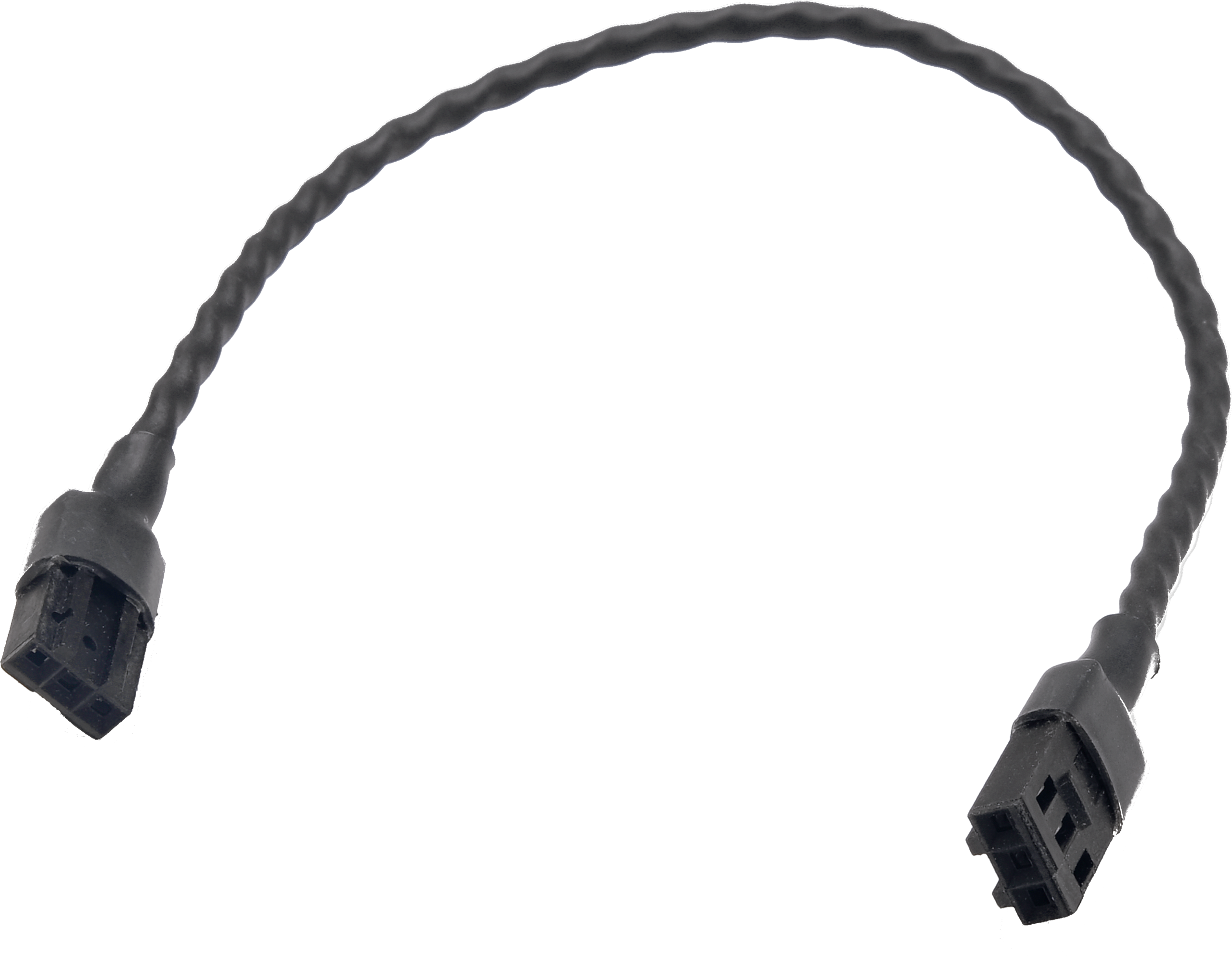
A316
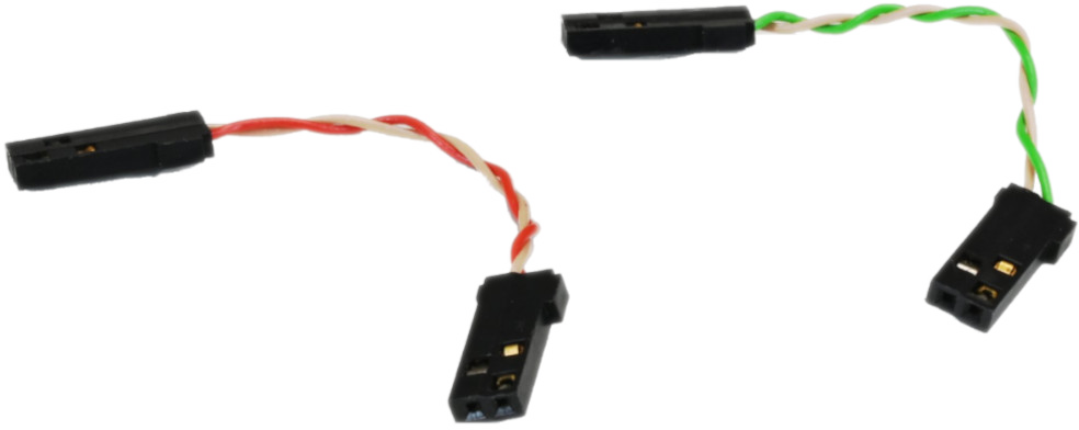
Cable assembly 2.54mm 2-pin header female - 5 cm
VX1720: Data Sheets

VX1720: Manuals
VX1720: Download
Guides
White Papers
Application Notes
Articles
Brochures / Flyers
Request a Quote

Footer

