-
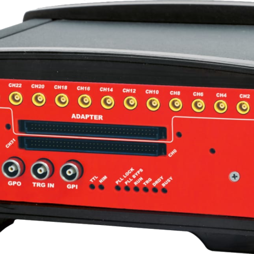
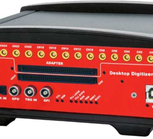
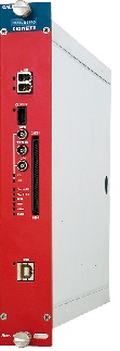
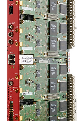
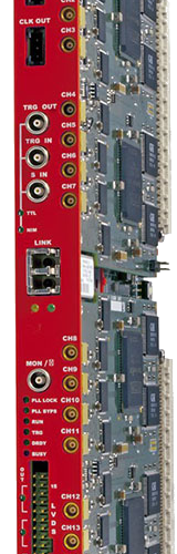
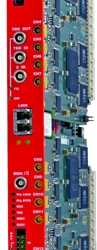
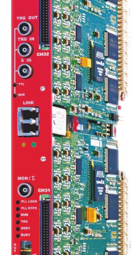
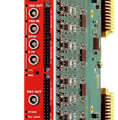
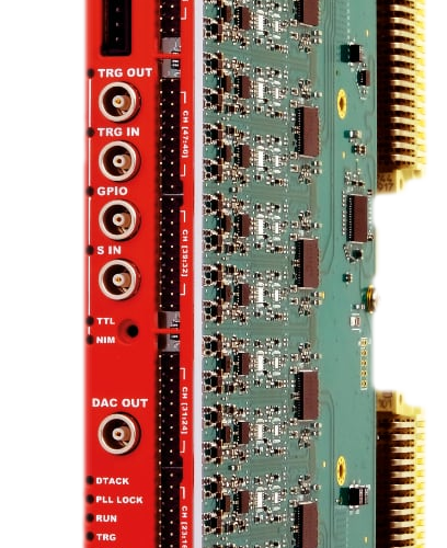
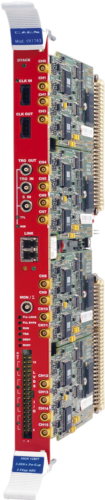
16-bit @ 125 MS/s ADC – TEST Prod 14:22
-
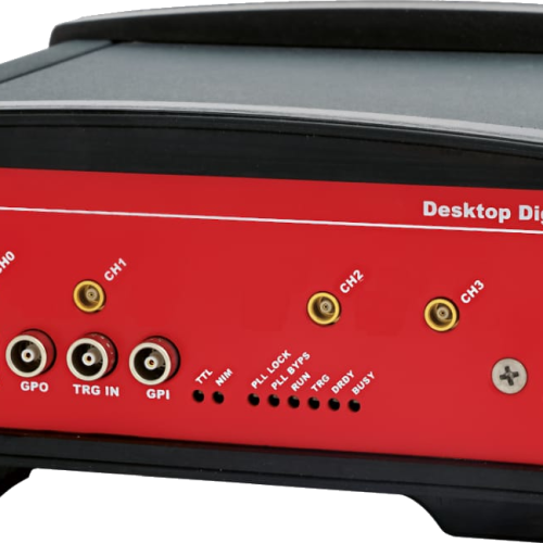
64 analog inputs, differential or single-ended, on four 2mm 40-pin header connectors
-
2Vpp input range, fixed Analog Gain x1
-
Fully supported by CoMPASS and WaveDump2 readout software
-
Open FPGA programming through graphical tool SCI-Compiler
-
Wide range of applications (from Neutrino Physics & Dark Matter to Nuclear and Particle Physics to Spectroscopic Imaging)
-
Suited for signals from Semiconductor Detectors coupled with CSPs (Si, HPGe) or scintillators coupled with PMTs (NaI, CsI)
-
On-board firmware selection for different acquisition modes:
-
Scope mode (simultaneous raw waveform acquisition on common trigger)
-
DPP-PHA mode (pulse height and time acquisition on independent channel self-triggers)
-
DPP-PSD mode (pulse shape discrimination and time acquisition on independent channel self-triggers)
-
Predisposition for other algorithms like zero suppression and data reduction
-
-
Multi-board synchronization and system building capabilities
-
Rack mount brackets included
-
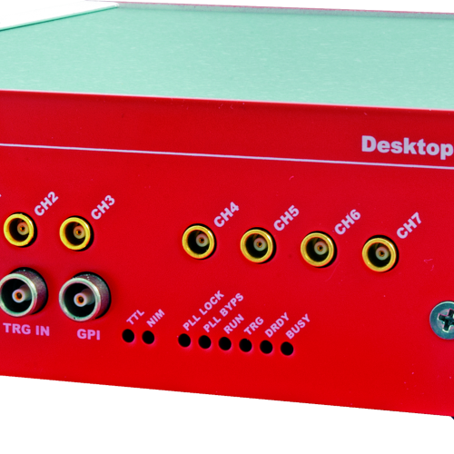
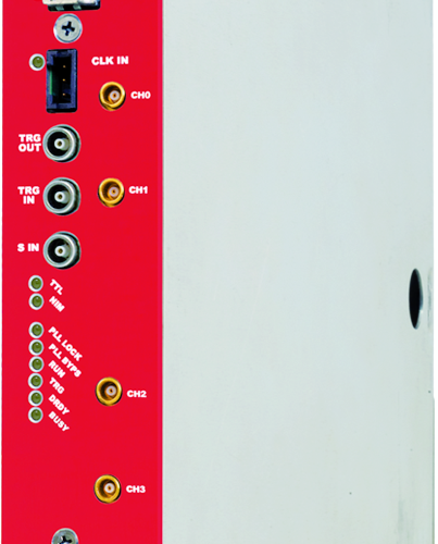
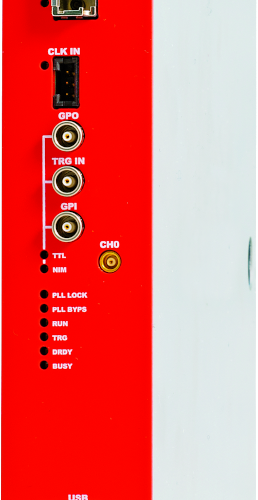
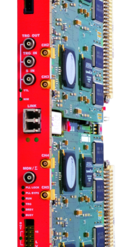
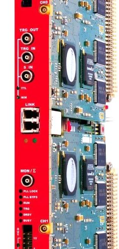
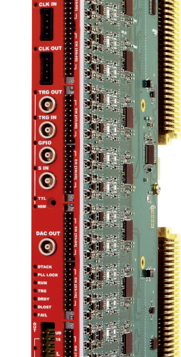
Front panel fully programmable I/Os (4 LEMO TTL/NIM and 16 LVDS)
-
Special 125MS/s 14bit DAC output (LEMO) for signal inspection, pulse generation, majority level
-
2.5GB of Total Acquisition memory (DDR4)
-
On-board Zynq® UltraScale +™ MPSoC integrating an Arm®-based CPU running Linux®
-
Multi Interface: USB-3.0 and 1/10 GbE or CONET Available on request optical link (switchable on the same socket)
-
SDK for embedded Arm and host PC

Analog
Digitizers
Digitizers Models
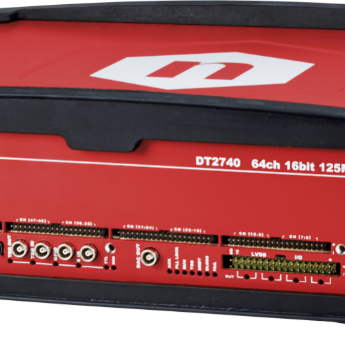
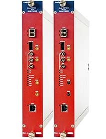
DT2740
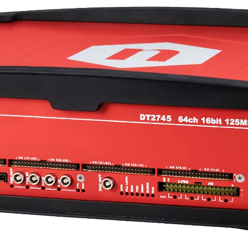
DT2745
-
16-bit @ 125 MS/s ADC
-
64 analog inputs, differential or single-ended, on four 2mm 40-pin header connectors
-
Software selectable Analog Gain up to x100
-
Open FPGA programming through graphical tool SCI-Compiler
-
Wide range of applications (from Neutrino Physics & Dark Matter to Nuclear and Particle Physics to Spectroscopic Imaging)
-
Suited for signals from Semiconductor Detectors coupled with CSPs (Si, HPGe) or scintillators coupled with PMTs (NaI, CsI)
-
On-board firmware selection for different acquisition modes:
-
Scope mode (simultaneous raw waveform acquisition on common trigger)
-
DPP-PHA mode (pulse height and time acquisition on independent channel self-triggers)
-
DPP-PSD mode (pulse shape discrimination and time acquisition on independent channel self-triggers)
-
Predisposition for other algorithms like zero suppression and data reduction
-
-
Multi-board synchronization and system building capabilities
-
Rack mount brackets included
-
Front panel fully programmable I/Os (4 LEMO TTL/NIM and 16 LVDS)
-
Special 125MS/s 14bit DAC output (LEMO) for signal inspection, pulse generation, majority level
-
2.5GB of Total Acquisition memory (DDR4)
-
On-board Zynq® UltraScale +™ MPSoC integrating an Arm®-based CPU running Linux®
-
Multi Interface: USB-3.0 and 1/10 GbE or CONET optical link (switchable on the same socket)
-
Fully supported by CoMPASS and WaveDump2 readout software (CoMPASS support is Available on request)
-
SDK for embedded Arm and host PC
-
Open FPGA architecture for pulse analysis algorithm customization
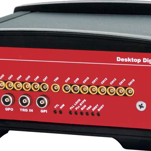
DT5720
-
12 bit 250 MS/s ADC
-
FPGA for real time Digital Pulse Processing:
-
Pulse Shape Discrimination (DPP-PSD)
-
Zero Suppression (Waveform Recording Firmware)
-
-
4/2 channels
-
MCX input (50 Ω, single ended)
-
2 Vpp single ended input range
-
16-bit programmable DC offset adjustment: ±1 V
-
Trigger Time stamps
-
Memory buffer: 1.25 MS/ch or 10 MS/ch
-
Programmable event size and pre-post trigger adjustment
-
Optical Link interface (CAEN proprietary protocol)
-
USB 2.0 interface
-
Firmware upgradeable via USB/Optical Link
-
Libraries, Demos (C and LabView) and Software tools for Windows and Linux
-
External AC-DC Power Supply Adapter (+12 V)
-
Dimensions: 154x50x164 mm3 (WxHxD)
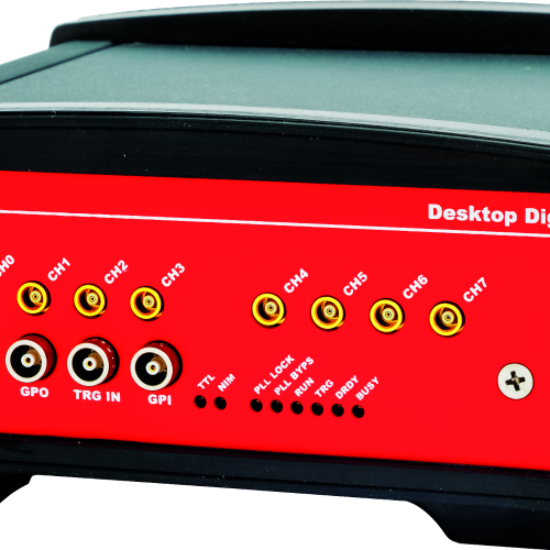
DT5724
-
14 bit @ 100 MS/s
-
Analog input on MCX coaxial connector (50 Ω, single-ended)
-
2/4 channels, Desktop module
-
2.25 Vpp single-ended input range (500 mVpp & 10 Vpp on request) with programmable DC offset
-
Sampling rate decimation factor (Waveform Recording firmware only)
-
Algorithms for Digital Pulse Processing:
-
Pulse Height Analysis (DPP-PHA)
-
Dynamic Acquisition Window (DPP-DAW)
-
Zero Suppression (Waveform Recording Firmware)
-
-
Time-stamped Waveform and List
-
USB and Optical Link communication interfaces
-
Multi-board synchronization features
-
Daisy chain capability
-
Compliant with CoMPASS, MC2Analyzer, DPP-DAW Demo Software, CAENScope, CAEN WaveDump, C and LabVIEW libraries

DT5725 / DT5725S
-
14-bit @ 250 MS/s
-
Analog inputs on MCX coaxial connectors
-
8 channels, Desktop module
-
0.5 and 2 Vpp selectable input dynamic range with programmable DC offset adjustment
-
Algorithms for Digital Pulse Processing
-
Pulse Height Analysis (DPP-PHA)
-
Pulse Shape Discrimination (DPP-PSD)
-
Zero Length Encoding (DPP-ZLEplus) – NEW
-
Dynamic Acquisition Window (DPP-DAW) – NEW
-
-
USB and Optical Link communication interfaces
-
Multi-board synchronization features
-
Daisy chain capability
-
Compliant with CoMPASS, MC2Analyzer, DPP-ZLEplus and DPP-DAW Demo Software, C and LabVIEW libraries
DT5730 / DT5730S
-
14-bit @ 500 MS/s
-
Analog inputs on MCX coaxial connectors
-
NSCLDAQ Supported (DPP-PSD and DPP-PHA only)
-
8 channels, Desktop module
-
0.5 and 2 Vpp selectable input dynamic range with programmable DC offset adjustment
-
Algorithms for Digital Pulse Processing (Free Trial)
-
Pulse Height Analysis (DPP-PHA)
-
Pulse Shape Discrimination (DPP-PSD)
-
Zero Length Encoding (DPP-ZLEplus) – NEW
-
Dynamic Acquisition Window (DPP-DAW) – NEW
-
-
USB and Optical Link communication interfaces
-
Multi-board synchronization features
-
Daisy chain capability
-
Compliant with CoMPASS, MC2Analyzer, DPP-ZLEplus and DPP-DAW Demo Software, C and LabVIEW libraries
DT5740
-
12 bit 62.5 MS/s ADC
-
32 / 16 channels
-
ERNI SMC Dual Row 68pin connector (32 channels)
-
Auxiliary ERNI SMC Dual Row 68pin connector
-
MCX connectors (16 channels by using auxiliary SMC)
-
2 Vpp single ended input range (10 Vpp also available)
-
16-bit programmable DC offset adjustment: ±1 V (±5 V)
-
Trigger Time stamps
-
Memory buffer: 192 kS/ch, up to 1024 events
-
FPGA for real-time data processing
-
Programmable event size and pre-post trigger adjustment
-
Optical Link interface (CAEN proprietary protocol)
-
USB 2.0 compliant interface
-
Firmware upgradeable via USB or Optical Link
-
Libraries, Demos (C and LabView) and Software tools for Windows and Linux
-
External AC-DC Power Supply Adapter (+12 V)
-
Dimensions: 154x50x164 mm3 (WxHxD)
DT5740D
-
12 bit 62.5 MS/s ADC
-
32 / 16 channels
-
ERNI SMC Dual Row 68pin connector (32 channels)
-
Auxiliary ERNI SMC Dual Row 68pin connector
-
MCX connectors (16 channels by using auxiliary SMC)
-
2 Vpp single ended input range
-
16-bit programmable DC offset adjustment: ±1 V
-
Trigger Time stamps
-
Memory buffer: 192 kS/ch, up to 1024 events
-
FPGA for real-time data processing:
-
Digital Charge to Digital Converter (DPP-QDC)
-
-
Programmable event size and pre-post trigger adjustment
-
Optical Link interface (CAEN proprietary protocol)
-
USB 2.0 compliant interface
-
Firmware upgradeable via USB or Optical Link
-
Caen DPP-QDC demo software (windows only) with C source file for developers
-
External AC-DC Power Supply Adapter (+12 V)
-
Dimensions: 154x50x164 mm3 (WxHxD)
DT5742
-
12 bit @ 5 GS/s, Desktop module
-
Switched Capacitor technology based on the DRS4 chip (designed at Paul Scherrer Institute)
-
1024 capacitor cells per channel (acquisition window of ~ 200 ns @ 5 GS/s)
-
-
5 GS/s, 2.5 GS/s, 1 GS/s, 750 MS/s software selectable sampling frequencies
-
16 analog input channels on MCX coaxial connectors
-
1 additional analog input (TR0):
-
fast (low latency) trigger
-
digitizable for high resolution timing (up to 50 ps)
-
-
1 Vpp input dynamic range (2 Vpp on request) with programmable DC offset adjustment
-
Dead-time due to conversion: 110 µs (analog inputs only), 181 µs (TR0 input)
-
Trigger modes:
-
External on TRG-IN connector; common to all groups
-
Fast (Low Latency) on TR0 connector; common to all groups
-
Self-trigger, combinations of channels over-threshold in logic OR; common to all groups
-
-
Memory buffer options: 128 events/ch; 1024 events/ch
-
USB and Optical Link communication interfaces
-
Demo software tools, C and LabVIEW libraries
DT5743
-
12-bit @ 3.2 GS/s, 1024 samples per event
-
Developed in collaboration with CEA/IRFU & CNRS/IN2P3/LAL and based on the SAMLONG chip
-
3.2, 1.6, 0.8, 0.4 GS/s software selectable sampling frequencies
-
Analog inputs on MCX coax. connectors
-
8 channels in a compact Desktop form factor
-
2.5 Vpp input dynamic range with programmable individual DC offset adj.
-
One discriminator per channel with programmable threshold
-
Adjustable post-trigger delay (up to 1.25 µs @ 3.2 GS/s)
-
Digital Memory buffer: 7 events/ch
-
1024 samples per channel (320 ns recorded time per event @ 3.2 GS/s)
-
Dead time due to event conversion: 125 µs (max. @ 1024 samples)
-
Real time hit counting independent of acquisition rate on each channel
-
On-board charge calculation for fast histogramming (user-defined integration window)
-
One embedded pulser per channel for test and reflectometry applications
-
Optical Link interface (CAEN proprietary protocol)
-
USB 2.0 compliant communication interface
-
A2818(PCI) / A3818 (PCIe) Controller available for handling up to 8/32 modules Daisy chained via Optical Link
-
Firmware upgradeable via USB/Optical Link
-
Fully controlled by the WaveCatcher readout software
-
Drivers and libraries for Windows and Linux 32/64-bit
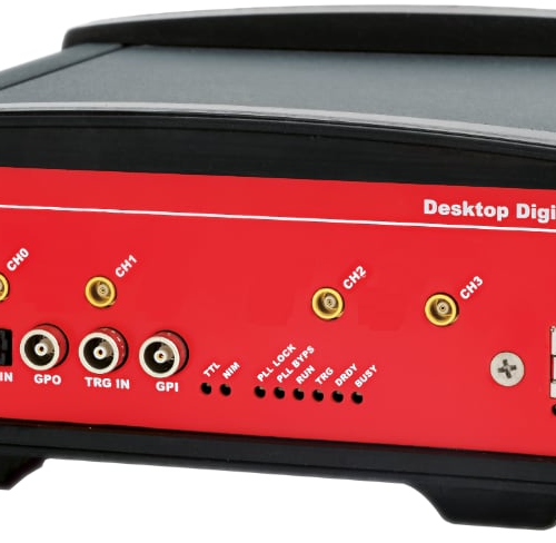
DT5751
-
10 bit @ 2 GS/s (interleaved) or 1 GS/s
-
Analog input on MCX coaxial connector (50 Ω, single-ended)
-
2-4 channels, Desktop module
-
1 Vpp input dynamic range (0.2 Vpp on request) with programmable DC offset
-
Algorithms for Digital Pulse Processing:
-
Pulse Shape Discrimination (DPP-PSD)
-
Zero Length Encoding (DPP-ZLEplus)
-
-
Time-stamped Waveform and List
-
USB and Optical Link communication interfaces
-
Multi-board synchronization features
-
Daisy chain capability
-
Compliant with CoMPASS, DPP-ZLEplus Demo Software, CAENScope, CAEN WaveDump, C and LabVIEW libraries
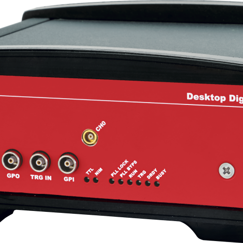
DT5761
-
10 bit @ 4 GS/s
-
Analog input on MCX coaxial connector (50 ohm, single ended)
-
1 channel, Desktop module
-
1 Vpp input dynamic range with programmable DC offset adjustment
-
Time-stamped Waveform Recorder
-
Memory buffer: 7.2 MS/ch
-
Programmable event size and post-trigger adjustment
-
USB and Optical Link communication interfaces
-
Multi-board synchronization features
-
Daisy chain capability
-
Compliant with CAEN WaveDump, C and LabVIEW Libraries
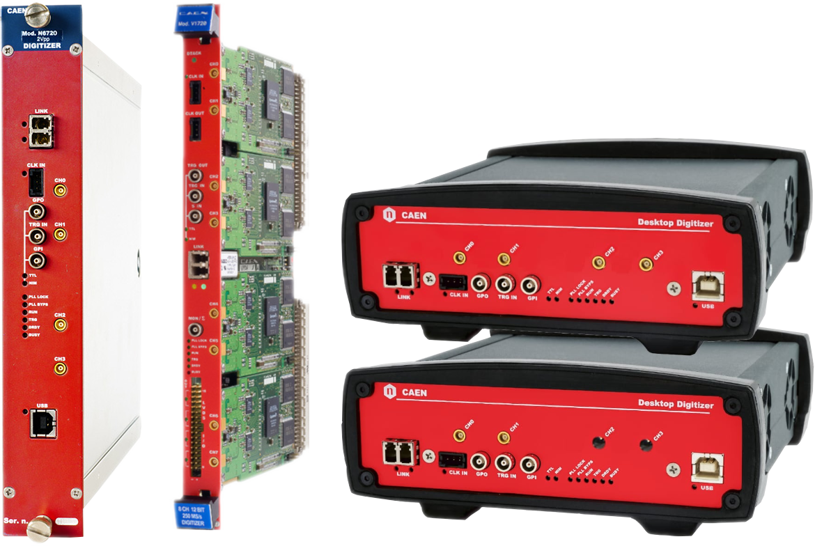
N6720
-
12 bit 250 MS/s ADC
-
FPGA for real time Digital Pulse Processing:
-
Pulse Shape Discrimination (DPP-PSD)
-
Zero Suppression (Waveform Recoding Firmware)
-
-
4/2 channels
-
MCX input (50 Ω, single ended)
-
2 Vpp single ended input range
-
16-bit programmable DC offset adjustment: ±1 V
-
Trigger Time stamps
-
Memory buffer: 1.25 MS/ch or 10 MS/ch
-
Programmable event size and pre-post trigger adjustment
-
Optical Link interface (CAEN proprietary protocol)
-
USB 2.0 interface
-
Firmware upgradeable via USB/Optical Link
-
Libraries, Demos (C and LabView) and Software tools for Windows and Linux
N6724
-
14 bit @ 100 MS/s
-
Analog input on MCX coaxial connector (50 Ω, single-ended)
-
2/4 channels, NIM module
-
2.25 Vpp single-ended input range (500 mVpp & 10 Vpp on request) with programmable DC offset
-
Sampling rate decimation factor (Waveform Recording firmware only)
-
Algorithms for Digital Pulse Processing:
-
Pulse Height Analysis (DPP-PHA)
-
Dynamic Acquisition Window (DPP-DAW)
-
Zero Suppression (Waveform Recording Firmware)
-
-
Time-stamped Waveform and List
-
USB and Optical Link communication interfaces
-
Multi-board synchronization features
-
Daisy chain capability
-
Compliant with CoMPASS, MC2Analyzer, DPP-DAW Demo Software, CAENScope, CAEN WaveDump, C and LabVIEW libraries
N6725 / N6725S
-
8 channels, 14-bit @ 250 MS/s
-
Analog inputs on MCX coaxial connectors
-
0.5 and 2 Vpp selectable input dynamic range with programmable DC offset adjustment
-
Algorithms for Digital Pulse Processing
-
Pulse Height Analysis (DPP-PHA)
-
Pulse Shape Discrimination (DPP-PSD)
-
Zero Length Encoding (DPP-ZLEplus) – NEW
-
Dynamic Acquisition Window (DPP-DAW) – NEW
-
-
USB and Optical Link communication interfaces
-
Multi-board synchronization features
-
Daisy chain capability
-
Compliant with CoMPASS, MC2Analyzer, DPP-ZLEplus and DPP-DAW Demo Software, C and LabVIEW libraries
N6730 / N6730S
-
14-bit @ 500 MS/s
-
Analog inputs on MCX coaxial connectors
-
NSCLDAQ Supported (DPP-PSD and DPP-PHA only)
-
8 channels, 1-unit wide NIM module
-
0.5 and 2 Vpp selectable input dynamic range with programmable DC offset adjustment
-
Algorithms for Digital Pulse Processing (Free Trial)
-
Pulse Height Analysis (DPP-PHA)
-
Pulse Shape Discrimination (DPP-PSD)
-
Zero Length Encoding (DPP-ZLEplus) –NEW
-
Dynamic Acquisition Window (DPP-DAW) –NEW
-
-
USB and Optical Link communication interfaces
-
Multi-board synchronization features
-
Daisy chain capability
-
Compliant with CoMPASS, MC2Analyzer, DPP-ZLEplus and DPP-DAW Demo Software, C and LabVIEW libraries
N6740
-
12 bit 62.5 MS/s ADC
-
32 channels (16 channels on LEMO connectors using A746D adapter)
-
ERNI SMC Dual Row 68pin connector (32 channels)
-
2 Vpp single ended input range (10 Vpp also available)
-
16-bit programmable DC offset adjustment: ±1 V (±5 V)
-
Trigger Time stamps
-
Memory buffer: 192 kS/ch, up to 1024 events
-
FPGA for real-time data processing
-
Programmable event size and pre-post trigger adjustment
-
Optical Link interface (CAEN proprietary protocol)
-
USB2.0 interface
-
Firmware upgradeable via USB/Optical Link
-
Libraries, Demos (C and LabView) and Software tools for Windows and Linux
N6740D
-
12 bit 62.5 MS/s ADC
-
32 channels (16 channels on LEMO connectors using A746D adapter)
-
ERNI SMC Dual Row 68 pin connector (32 channels)
-
2 Vpp single ended input range
-
16-bit programmable DC offset adjustment: ±1 V
-
Trigger Time stamps
-
Memory buffer: 192 kS/ch, up to 1024 events
-
FPGA for real-time data processing:
-
Digital Charge to Digital Converter (DPP-QDC)
-
-
Programmable event size and pre-post trigger adjustment
-
Optical Link interface (CAEN proprietary protocol)
-
USB2.0 interface
-
Firmware upgradeable via USB/Optical Link
-
Libraries, Demos (C and LabView) and Software tools for Windows and Linux
N6742
-
12 bit @ 5 GS/s, 1-unit wide NIM module
-
Switched Capacitor technology based on the DRS4 chip (designed at Paul Scherrer Institute)
-
1024 capacitor cells per channel (acquisition window of ~ 200 ns @ 5 GS/s)
-
-
5 GS/s, 2.5 GS/s, 1 GS/s, 750 MS/s software selectable sampling frequencies
-
16 analog input channels on MCX coaxial connectors
-
1 additional analog input (TR0):
-
fast (low latency) trigger
-
digitizable for high resolution timing (up to 50 ps)
-
-
1 Vpp input dynamic range (2 Vpp on request) with programmable DC offset adjustment
-
Dead-time due to conversion: 110 µs (analog inputs only), 181 µs (TR0 input)
-
Trigger modes:
-
External on TRG-IN connector; common to all groups
-
Fast (Low Latency) on TR0 connector; common to all groups
-
Self-trigger, combinations of channels over-threshold in logic OR; common to all groups
-
-
Memory buffer options: 128 events/ch; 1024 events/ch
-
USB and Optical Link communication interfaces
-
Demo software tools, C and LabVIEW libraries
N6743
-
12-bit @ 3.2 GS/s, 1024 samples per event
-
Developed in collaboration with CEA/IRFU & CNRS/IN2P3/LAL and based on the SAMLONG chip
-
3.2, 1.6, 0.8, 0.4 GS/s software selectable sampling frequencies
-
Analog inputs on MCX coax. connectors
-
8 channels in a 1-unit NIM form factor
-
2.5 Vpp input dynamic range with programmable individual DC offset adj.
-
One discriminator per channel with programmable threshold
-
Adjustable post-trigger delay (up to 1.25 µs @ 3.2 GS/s)
-
Digital Memory buffer: 7 events/ch
-
1024 samples per channel (320 ns recorded time per event @ 3.2 GS/s)
-
Dead time due to event conversion: 125 µs (max. @ 1024 samples)
-
Real time hit counting independent of acquisition rate on each channel
-
On-board charge calculation for fast histogramming (user-defined integration window)
-
One embedded pulser per channel for test and reflectometry applications
-
Optical Link interface (CAEN proprietary protocol)
-
USB 2.0 compliant communication interface
-
A2818(PCI) / A3818 (PCIe) Controller available for handling up to 8/32 modules Daisy chained via Optical Link
-
Firmware upgradeable via USB/Optical Link
-
Fully controlled by the WaveCatcher readout software
-
Drivers and libraries for Windows and Linux 32/64-bit
N6751
-
10 bit @ 2 GS/s (interleaved) or 1 GS/s
-
Analog input on MCX coaxial connector (50 Ω, single-ended)
-
2-4 channels, NIM module
-
1 Vpp input dynamic range (0.2 Vpp on request) with programmable DC offset
-
Algorithms for Digital Pulse Processing:
-
Pulse Shape Discrimination (DPP-PSD)
-
Zero Length Encoding (DPP-ZLEplus)
-
-
Time-stamped Waveform and List
-
USB and Optical Link communication interfaces
-
Multi-board synchronization features
-
Daisy chain capability
-
Compliant with CoMPASS, DPP-ZLEplus Demo Software, CAENScope, CAEN WaveDump, C and LabVIEW libraries
N6761
-
10 bit @ 4 GS/s
-
Analog input on MCX coaxial connector (50 Ω, single ended)
-
1 channel, Desktop module
-
1 Vpp input dynamic range with programmable DC offset adjustment
-
Time-stamped Waveform Recorder
-
Memory buffer: 7.2 MS/ch
-
Programmable event size and post-trigger adjustment
-
USB and Optical Link communication interfaces
-
Multi-board synchronization features
-
Daisy chain capability
-
Compliant with CAEN WaveDump, C and LabVIEW Libraries
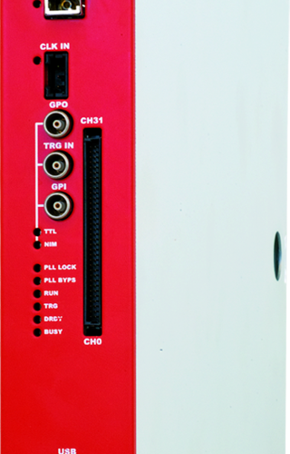
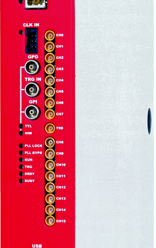
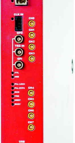
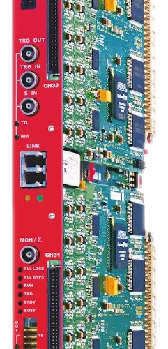
R5560
-
128 channels, 14-bit @125 MS/s Digitizer
-
Based on powerful Xilinx Zynq-7000 SoC with open FPGA
-
2U, 19” Rackmount unit with automatic fan control
-
Full-featured readout system for the readout of large arrays of detector (PMTs, segmented HPGe, Gas Tubes, …)
-
Specifically designed for the readout of position-sensitive 3He tubes in combination with R1443 preamplifier
-
2 Vpp input dynamic
-
Fully supported by SCI-Compiler for easy FPGA programming (Firmware runtime license included onboard)
-
Easily scalable
-
Board-to-board synchronization with a single CAT5e cable.
-
Configurable digital I/Os to interface with external systems
-
Maximum flexibility: USB3.0, Ethernet, and Optical Link (OPTIONAL) connectivity, to support remote management as well as extreme fast data flow
-
2.4” touch screen display for quick configuration and status control
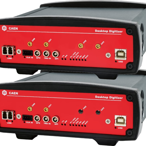
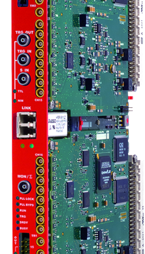
V1720
-
12 bit 250 MS/s ADC
-
FPGA for real time Digital Pulse Processing:
-
Pulse Shape Discrimination (DPP-PSD)
-
Zero Suppression (Waveform Recording Firmware)
-
-
8 channels
-
2 Vpp input range (single ended)
-
16-bit programmable DC offset adjustment: ±1 V
-
Trigger Time stamps
-
Memory buffer: 1.25 or 10 MS/ch, up to 1024 events
-
Programmable event size and pre-post trigger adjustment
-
Analog Sum/Majority and digital over/under threshold flags for Global Trigger logic
-
Front panel clock In/Out available for multiboard synchronisation (direct feed through or PLL based synthesis)
-
16 programmable LVDS I/Os
-
Optical Link interface (CAEN proprietary protocol)
-
VME64X compliant interface
-
Firmware upgradeable via VME/Optical Link
-
A2818 (PCI) / A3818 (PCIe) Controller available for handling up to 8/32 modules Daisy chained via Optical Link
-
Libraries, Demos (C and LabView) and Software tools for Windows and Linux
V1724
-
14 bit @ 100 MS/s
-
Analog input on MCX coaxial connector (50 Ω, single-ended)
-
8 channels, 1-unit wide 6U VME module
-
2.25 Vpp single-ended input range (500 mVpp / 10 Vpp on request) with programmable DC offset
-
Sampling rate decimation factor (Waveform Recording firmware only)
-
Algorithms for Digital Pulse Processing:
-
Pulse Height Analysis (DPP-PHA)
-
Dynamic Acquisition Window (DPP-DAW)
-
Zero Suppression (Waveform Recording Firmware)
-
-
Time-stamped Waveform and List
-
VME64 (VME64X compliant) and Optical Link communication interfaces
-
Multi-board synchronization features
-
Daisy chain capability
-
Compliant with CoMPASS, MC2Analyzer, DPP-DAW Demo Software, CAENScope, CAEN WaveDump, C and LabVIEW libraries
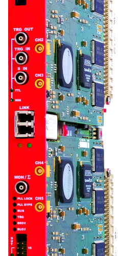
V1725 / V1725S
-
14-bit @ 250 MS/s
-
Analog inputs on MCX coaxial connectors
-
16/8 channels, 1-unit wide 6U VME64 module
-
0.5 and 2 Vpp selectable input dynamic range with programmable DC offset adjustment
-
Algorithms for Digital Pulse Processing
-
Pulse Height Analysis (DPP-PHA)
-
Pulse Shape Discrimination (DPP-PSD)
-
Zero Length Encoding (DPP-ZLEplus)
-
Dynamic Acquisition Window (DPP-DAW)
-
-
VME64 (VME64X compliant) and Optical Link communication interfaces
-
Multi-board synchronization features
-
16 programmable LVDS I/Os
-
Daisy chain capability
-
Compliant with CoMPASS, MC2Analyzer, DPP-ZLEplus and DPP-DAW Demo Software, C and LabVIEW libraries
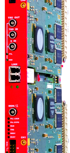
V1730 / V1730S
-
14-bit @ 500 MS/s
-
Analog inputs on MCX coaxial connectors
-
NSCLDAQ Supported (DPP-PSD and DPP-PHA only)
-
16/8 channels, 1-unit wide 6U VME64 module
-
0.5 and 2 Vpp selectable input dynamic range with programmable DC offset adjustment
-
Algorithms for Digital Pulse Processing (Free Trial)
-
Pulse Height Analysis (DPP-PHA)
-
Pulse Shape Discrimination (DPP-PSD)
-
Zero Length Encoding (DPP-ZLEplus)
-
Dynamic Acquisition Window (DPP-DAW)
-
-
VME64 (VME64X compliant) and Optical Link communication interfaces
-
Multi-board synchronization features
-
16 programmable LVDS I/Os
-
Daisy chain capability
-
Compliant with CoMPASS, MC2Analyzer, DPP-ZLEplus and DPP-DAW Demo Software, C and LabVIEW libraries
V1740D
-
12 bit 62.5 MS/s ADC
-
64 channels
-
Two ERNI SMC Dual Row 68pin connectors (32 + 32 channels)
-
2 Vpp single ended input range
-
16-bit programmable DC offset adjustment: ±1 V
-
Trigger Time stamps
-
Memory buffer: 192 kS/ch, up to 1024 events
-
FPGA for real-time data processing:
-
Digital Charge to Digital Converter (DPP-QDC)
-
-
Programmable event size and pre-post trigger adjustment
-
Analog Sum/Majority and digital over/under threshold flags for Global Trigger logic
-
Front panel clock In/Out available for multiboard synchronisation (direct feed through or PLL based synthesis)
-
16 programmable LVDS I/Os
-
Optical Link interface (CAEN proprietary protocol)
-
VME64X compliant interface
-
A2818 (PCI) / A3818 (PCIe) Controller available for handling up to 8/32 modules Daisy chained via Optical Link
-
Firmware upgradeable via VME/Optical Link
-
Libraries, Demos (C and LabView) and Software tools for Windows and Linux
V1742
-
12 bit @ 5 GS/s, 1-unit wide 6U VME64 module
-
Switched Capacitor technology based on the DRS4 chip (designed at Paul Scherrer Institute)
-
1024 capacitor cells per channel (acquisition window of ~ 200 ns @ 5 GS/s)
-
-
5 GS/s , 2.5 GS/s, 1 GS/s, 750 MS/s software selectable sampling frequencies
-
32 analog input channels on MCX coaxial connectors
-
2 additional analog inputs (TR0 and TR1):
-
fast (low latency) trigger
-
digitizable for high resolution timing (up to 50 ps)
-
-
1 Vpp input dynamic range (2 Vpp on request) with programmable DC offset adjustment
-
Dead-time due to conversion: 110 µs (analog inputs only), 181 µs (TR0, TR1 inputs)
-
Trigger modes:
-
External on TRG-IN connector; common to all groups
-
Fast (Low Latency) on TR0 and TR1 connectors; common to couples of groups
-
Self-trigger, combinations of channels over-threshold in logic OR; common to couples of groups
-
-
Memory buffer options: 128 events/ch; 1024 events/ch
-
VME64 (VME64X compliant) and Optical Link communication interfaces
-
Multi-board synchronization features
-
16 programmable LVDS I/Os
-
Demo software tools, C and LabVIEW libraries
V1743
-
12-bit @ 3.2 GS/s, 1024 samples per event
-
Developed in collaboration with CEA/IRFU & CNRS/IN2P3/LAL and based on the SAMLONG chip
-
3.2, 1.6, 0.8, 0.4 GS/s software selectable sampling frequencies
-
Analog inputs on MCX coax. connectors
-
16 channels in 1-unit VME 6U form factor
-
2.5 Vpp input dynamic range with programmable individual DC offset adj.
-
One discriminator per channel with programmable threshold
-
Adjustable post-trigger delay (up to 1.25 µs @ 3.2 GS/s)
-
Digital Memory buffer: 7 events/ch
-
1024 samples per channel (320 ns recorded time per event @ 3.2 GS/s)
-
Dead time due to event conversion: 125 µs (max. @ 1024 samples)
-
Real time hit counting independent of acquisition rate on each channel
-
On-board charge calculation for fast histogramming (user-defined integration window)
-
One embedded pulser per channel for test and reflectometry applications
-
Optical Link interface (CAEN proprietary protocol)
-
VME64X-compliant interface
-
A2818(PCI) / A3818 (PCIe) Controller available for handling up to 8/32 modules Daisy chained via Optical Link
-
Firmware upgradeable via VMEbus/Optical Link
-
Multi-board synchronization features
-
16 programmable LVDS I/Os
-
Fully controlled by the WaveCatcher readout software
-
Drivers and libraries for Windows and Linux 32/64-bit
V1751
-
10 bit @ 2 GS/s (interleaved) or 1 GS/s
-
Analog input on MCX coaxial connector (50 Ω, single-ended)
-
4-8 channels, 1-unit wide 6U VME64 module
-
1 Vpp input dynamic range (0.2 Vpp on request) with programmable DC offset
-
Algorithms for Digital Pulse Processing:
-
Pulse Shape Discrimination (DPP-PSD)
-
Zero Length Encoding (DPP-ZLEplus)
-
-
Time-stamped Waveform and List
-
VME64 (VME64X compliant) and Optical Link communication interfaces
-
Multi-board synchronization features
-
16 programmable LVDS I/Os
-
Daisy chain capability
-
Compliant with CoMPASS, DPP-ZLEplus Demo Software, CAENScope, CAEN WaveDump, C and LabVIEW libraries
V1761
-
10-bit @ 4 GS/s
-
Analog inputs on MCX coaxial connectors (50 Ω, single-ended)
-
2 channels, 1-unit wide 6U VME64 module
-
1 Vpp input dynamic range with programmable DC offset adjustment
-
Time-stamped Waveform Recorder
-
Memory buffer: 7.2 MS/ch or 57.6 MS/ch size
-
Programmable event size and post-trigger adjustment
-
VME64 (VME64X compliant) and Optical Link communication interfaces
-
Multi-board synchronization features
-
16 programmable LVDS I/Os
-
Daisy chain capability
-
Compliant with CAEN WaveDump, C and LabVIEW Libraries
V2740
-
16 bit @ 125 MS/s ADC
-
64 analog inputs, differential or single-ended, on four 2mm 40-pin header connectors
-
2Vpp input range, fixed Analog Gain x1
-
DT2740 desktop form factor also available
-
Open FPGA programming through graphical tool SCI-Compiler
-
Wide range of applications (from Neutrino Physics & Dark Matter to Nuclear and Particle Physics to Spectroscopic Imaging)
-
Suited for signals from Semiconductor Detectors coupled with CSPs (Si, HPGe) or scintillators coupled with PMTs (NaI, CsI)
-
On-board firmware selection for different acquisition modes:
-
Scope mode (simultaneous raw waveform acquisition on common trigger)
-
DPP-PHA mode (pulse height and time acquisition on independent channel self-triggers)
-
DPP-PSD mode (pulse shape discrimination and time acquisition on independent channel self-triggers)
-
Predisposition for other algorithms like zero suppression and data reduction
-
-
Multi-board synchronization and system building capabilities
-
Front panel fully programmable I/Os (4 LEMO TTL/NIM and 16 LVDS)
-
Special 125 MS/s 14bit DAC output (LEMO) for signal inspection, pulse generation, majority level
-
2.5GB of Total Acquisition memory (DDR4)
-
On-board Zynq® UltraScale+™ MPSoC integrating an Arm®-based CPU running Linux®
-
Multi Interface: USB-3.0 and 1/10 GbE or CONET Available on request optical link (switchable on the same socket)
-
SDK for embedded Arm and host PC
-
Open FPGA architecture for pulse analysis algorithm customization
V2745
-
16 bit @ 125 MS/s ADC
-
64 analog inputs, differential or single-ended, on four 2mm 40-pin header connectors
-
Software selectable Analog Gain up to x100
-
DT2745 desktop form factor also available
-
Open FPGA programming through graphical tool SCI-Compiler
-
Wide range of applications (from Neutrino Physics & Dark Matter to Nuclear and Particle Physics to Spectroscopic Imaging)
-
Suited for signals from Semiconductor Detectors coupled with CSPs (Si, HPGe) or scintillators coupled with PMTs (NaI, CsI)
-
On-board firmware selection for different acquisition modes:
-
Scope mode (simultaneous raw waveform acquisition on common trigger)
-
DPP-PHA mode (pulse height and time acquisition on independent channel self-triggers)
-
DPP-PSD mode (pulse shape discrimination and time acquisition on independent channel self-triggers)
-
Predisposition for other algorithms like zero suppression and data reduction
-
-
Multi-board synchronization and system building capabilities
-
Front panel fully programmable I/Os (4 LEMO TTL/NIM and 16 LVDS)
-
Special 125MS/s 14bit DAC output (LEMO) for signal inspection or trigger sum
-
On-board Xilinx Zynq® UltraScale+™ FPGA with embedded Linux-based ARM processor
-
2.5GB of Total Acquisition memory (DDR4)
-
Multi Interface: USB-3.0 and 1/10 GbE or CONET optical link (switchable on the same socket)
-
Fully supported by CoMPASS and WaveDump2 readout software
-
SDK for embedded Arm and host PC
-
Open FPGA
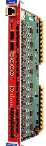
VX1720
-
12 bit 250 MS/s ADC
-
FPGA for real time Digital Pulse Processing:
-
Pulse Shape Discrimination (DPP-PSD)
-
Zero Suppression (Waveform Recording Firmware)
-
-
8 channels
-
2 Vpp input range (single ended)
-
16-bit programmable DC offset adjustment: ±1 V
-
Trigger Time stamps
-
Memory buffer: 1.25 or 10 MS/ch, up to 1024 events
-
Programmable event size and pre-post trigger adjustment
-
Analog Sum/Majority and digital over/under threshold flags for Global Trigger logic
-
Front panel clock In/Out available for multiboard synchronisation (direct feed through or PLL based synthesis)
-
16 programmable LVDS I/Os
-
VME64X compliant interface
-
Optical Link interface (CAEN proprietary protocol)
-
A2818 (PCI) / A3818 (PCIe) Controller available for handling up to 8/32 modules Daisy chained via Optical Link
-
Firmware upgradeable via VME/Optical Link
-
Libraries, Demos (C and LabView) and Software tools for Windows and Linux
VX1724
-
14 bit @ 100 MS/s
-
Analog input on MCX coaxial connector (50 Ω, single-ended)
-
8 channels, 1-unit wide 6U VME64X module
-
2.25 Vpp single-ended input range (500 mVpp & 10 Vpp on request) with programmable DC offset
-
Sampling rate decimation factor (Waveform Recording firmware only)
-
Algorithms for Digital Pulse Processing:
-
Pulse Height Analysis (DPP-PHA)
-
Dynamic Acquisition Window (DPP-DAW)
-
Zero Suppression (Waveform Recording Firmware)
-
-
Time-stamped Waveform and List
-
VME64X and Optical Link communication interfaces
-
Multi-board synchronization features
-
Daisy chain capability
-
Compliant with CoMPASS, MC2Analyzer, DPP-DAW Demo Software, CAENScope, CAEN WaveDump, C and LabVIEW libraries
VX1725 / VX1725S
-
14-bit @ 250 MS/s
-
Analog inputs on MCX coaxial connectors
-
16/8 channels, 1-unit wide 6U VME64 module
-
0.5 and 2 Vpp selectable input dynamic range with programmable DC offset adjustment
-
Algorithms for Digital Pulse Processing
-
Pulse Height Analysis (DPP-PHA)
-
Pulse Shape Discrimination (DPP-PSD)
-
Zero Length Encoding (DPP-ZLEplus) – NEW
-
Dynamic Acquisition Window (DPP-DAW) – NEW
-
-
VME64X and Optical Link communication interfaces
-
Multi-board synchronization features
-
16 programmable LVDS I/Os
-
Daisy chain capability
-
Compliant with CoMPASS, MC2Analyzer, DPP-ZLEplus and DPP-DAW Demo Software, C and LabVIEW libraries
VX1730 / VX1730S
-
14-bit @ 500 MS/s
-
Analog inputs on MCX coaxial connectors
-
NSCLDAQ Supported (DPP-PSD and DPP-PHA only)
-
16/8 channels, 1-unit wide 6U VME64X module
-
0.5 and 2 Vpp selectable input dynamic range with programmable DC offset adjustment
-
Algorithms for Digital Pulse Processing (Free Trial)
-
Pulse Height Analysis (DPP-PHA)
-
Pulse Shape Discrimination (DPP-PSD)
-
Zero Length Encoding (DPP-ZLEplus) – NEW
-
Dynamic Acquisition Window (DPP-DAW) – NEW
-
-
VME64X and Optical Link communication interfaces
-
Multi-board synchronization features
-
16 programmable LVDS I/Os
-
Daisy chain capability
-
Compliant with CoMPASS, MC2Analyzer, DPP-ZLEplus and DPP-DAW Demo Software, C and LabVIEW libraries

VX1740
-
12 bit 62.5 MS/s ADC
-
64 channels
-
Two ERNI SMC Dual Row 68pin connectors (32 + 32 channels)
-
2 Vpp single ended input range (10 Vpp also available)
-
16-bit programmable DC offset adjustment: ±1 V (±5 V)
-
Trigger Time stamps
-
Memory buffer: 192 kS/ch or 1.5 MS/ch, up to 1024 events
-
FPGA for real-time data processing
-
Programmable event size and pre-post trigger adjustment
-
Analog Sum/Majority and digital over/under threshold flags for Global Trigger logic
-
Front panel clock In/Out available for multiboard synchronisation (direct feed through or PLL based synthesis)
-
16 programmable LVDS I/Os
-
Optical Link interface (CAEN proprietary protocol)
-
VME64X compliant interface
-
A2818(PCI) / A3818 (PCIe) Controller available for handling up to 8/32 modules Daisy chained via Optical Link
-
Firmware upgradeable via VME/Optical Link
-
Libraries, Demos (C and LabView) and Software tools for Windows and Linux
VX1740D
-
12 bit 62.5 MS/s ADC
-
64 channels
-
Two ERNI SMC Dual Row 68pin connectors (32 + 32 channels)
-
2 Vpp single ended input range
-
16-bit programmable DC offset adjustment: ±1
-
Trigger Time stamps
-
Memory buffer: 192 kS/ch, up to 1024 events
-
FPGA for real-time data processing:
-
Digital Charge to Digital Converter (DPP-QDC)
-
-
Programmable event size and pre-post trigger adjustment
-
Analog Sum/Majority and digital over/under threshold flags for Global Trigger logic
-
Front panel clock In/Out available for multiboard synchronisation (direct feed through or PLL based synthesis)
-
16 programmable LVDS I/Os
-
Optical Link interface (CAEN proprietary protocol)
-
VME64X compliant interface
-
A2818(PCI) / A3818 (PCIe) Controller available for handling up to 8/32 modules Daisy chained via Optical Link
-
Firmware upgradeable via VME/Optical Link
-
Libraries, Demos (C and LabView) and Software tools for Windows and Linux
VX1742
-
12 bit @ 5 GS/s, 1-unit wide 6U VME64 module
-
Switched Capacitor technology based on the DRS4 chip (designed at Paul Scherrer Institute)
-
1024 capacitor cells per channel (acquisition window of ~ 200 ns @ 5 GS/s)
-
-
5 GS/s, 2.5 GS/s, 1 GS/s, 750 MS/s software selectable sampling frequencies
-
32 analog input channels on MCX coaxial connectors
-
2 additional analog inputs (TR0 and TR1):
-
fast (low latency) trigger
-
digitizable for high resolution timing (up to 50 ps)
-
-
1 Vpp input dynamic range (2 Vpp on request) with programmable DC offset adjustment
-
Dead-time due to conversion: 110 µs (analog inputs only), 181 µs (TR0, TR1 inputs)
-
Trigger modes:
-
External on TRG-IN connector; common to all groups
-
Fast (Low Latency) on TR0 and TR1 connectors; common to couples of groups
-
Self-trigger, combinations of channels over-threshold in logic OR; common to couples of groups
-
-
Memory buffer options: 128 events/ch; 1024 events/ch
-
VME64 (VME64X compliant) and Optical Link communication interfaces
-
Multi-board synchronization features
-
16 programmable LVDS I/Os
-
Demo software tools, C and LabVIEW libraries
VX1743
-
12-bit @ 3.2 GS/s, 1024 samples per event
-
Developed in collaboration with CEA/IRFU & CNRS/IN2P3/LAL and based on the SAMLONG chip
-
3.2, 1.6, 0.8, 0.4 GS/s software selectable sampling frequencies
-
Analog inputs on MCX coax. connectors
-
16 channels in 1-unit VME64X 6U form factor
-
2.5 Vpp input dynamic range with programmable individual DC offset adj.
-
One discriminator per channel with programmable threshold
-
Adjustable post-trigger delay (up to 1.25 µs @ 3.2 GS/s)
-
Digital Memory buffer: 7 events/ch
-
1024 samples per channel (320 ns recorded time per event @ 3.2 GS/s)
-
Dead time due to event conversion: 125 µs (max. @ 1024 samples)
-
Real time hit counting independent of acquisition rate on each channel
-
On-board charge calculation for fast histogramming (user-defined integration window)
-
One embedded pulser per channel for test and reflectometry applications
-
Optical Link interface (CAEN proprietary protocol)
-
VME64X-compliant interface
-
A2818 (PCI) / A3818 (PCIe) Controller available for handling up to 8/32 modules Daisy chained via Optical Link
-
Firmware upgradeable via VMEbus/Optical Link
-
Multi-board synchronization features
-
16 programmable LVDS I/Os
-
Fully controlled by the WaveCatcher readout software
-
Drivers and libraries for Windows and Linux 32/64-bit
VX1751
-
10 bit @ 2 GS/s (interleaved) or 1 GS/s
-
Analog input on MCX coaxial connector (50 Ω, single-ended)
-
4-8 channels, 1-unit wide 6U VME64X module
-
1 Vpp input dynamic range (0.2 Vpp on request) with programmable DC offset
-
Algorithms for Digital Pulse Processing:
-
Pulse Shape Discrimination (DPP-PSD)
-
Zero Length Encoding (DPP-ZLEplus)
-
-
Time-stamped Waveform and List
-
VME64X and Optical Link communication interfaces
-
Multi-board synchronization features
-
16 programmable LVDS I/Os
-
Daisy chain capability
-
Compliant with CoMPASS, DPP-ZLEplus Demo Software, CAENScope, CAEN WaveDump, C and LabVIEW libraries
VX1761
-
10-bit @ 4 GS/s
-
Analog inputs on MCX coaxial connectors (50 Ω, single-ended)
-
2 channels, 1-unit wide 6U VME64X module
-
1 Vpp input dynamic range with programmable DC offset adjustment
-
Time-stamped Waveform Recorder
-
Memory buffer: 7.2 MS/ch or 57.6 MS/ch size
-
Programmable event size and post-trigger adjustment
-
VME64 (VME64X compliant) and Optical Link communication interfaces
-
Multi-board synchronization features
-
16 programmable LVDS I/Os
-
Daisy chain capability
-
Compliant with CAEN WaveDump, C and LabVIEW Libraries
VX2740
-
16 bit @ 125 MS/s ADC
-
64 analog inputs, differential or single-ended, on four 2mm 40-pin header connectors
-
2Vpp input range, fixed Analog Gain x1
-
DT2740 desktop form factor also available
-
Open FPGA programming through graphical tool SCI-Compiler
-
Wide range of applications (from Neutrino Physics & Dark Matter to Nuclear and Particle Physics to Spectroscopic Imaging)
-
Suited for signals from Semiconductor Detectors coupled with CSPs (Si, HPGe) or scintillators coupled with PMTs (NaI, CsI)
-
On-board firmware selection for different acquisition modes:
-
Scope mode (simultaneous raw waveform acquisition on common trigger)
-
DPP-PHA mode (pulse height and time acquisition on independent channel self-triggers)
-
DPP-PSD mode (pulse shape discrimination and time acquisition on independent channel self-triggers)
-
Predisposition for other algorithms like zero suppression and data reduction
-
-
Fully supported by CoMPASS and WaveDump2 readout software and SCI-Compiler Firmware Generator
-
Multi-board synchronization and system building capabilities
-
Front panel fully programmable I/Os (4 LEMO TTL/NIM and 16 LVDS)
-
Special 125MS/s 14bit DAC output (LEMO) for signal inspection, pulse generation, majority level
-
2.5GB of Total Acquisition memory (DDR4)
-
On-board Zynq® UltraScale+™ MPSoC integrating an Arm®-based CPU running Linux®
-
Multi Interface: USB-3.0 and 1/10 GbE or CONET Available on request optical link (switchable on the same socket)
-
SDK for embedded Arm and host PC
-
Open FPGA architecture for pulse analysis algorithm customization
VX2745
-
16 bit @ 125 MS/s ADC
-
64 analog inputs, differential or single-ended, with programmable gain
-
Four 2mm 40-pin header connectors
-
DT2745 desktop form factor also available
-
Open FPGA programming through graphical tool SCI-Compiler
-
Wide range of applications (from Neutrino Physics & Dark Matter to Nuclear and Particle Physics to Spectroscopic Imaging)
-
Suited for signals from Semiconductor Detectors coupled with CSPs (Si, HPGe) or scintillators coupled with PMTs (NaI, CsI)
-
On-board firmware selection for different acquisition modes:
-
Scope mode (simultaneous raw waveform acquisition on common trigger)
-
DPP-PHA mode (pulse height and time acquisition on independent channel self-triggers)
-
DPP-PSD mode (pulse shape discrimination and time acquisition on independent channel self-triggers)
-
Predisposition for other algorithms like zero suppression and data reduction
-
-
Multi-board synchronization and system building capabilities
-
Front panel fully programmable I/Os (4 LEMO TTL/NIM and 16 LVDS)
-
Special 125MS/s 14bit DAC output (LEMO) for signal inspection or trigger sum
-
On-board Xilinx Zynq® UltraScale+™ FPGA with embedded Linux-based ARM processor
-
2.5GB of Total Acquisition memory (DDR4)
-
USB 3.0 type-C and 1/10 Gigabit Ethernet or optional CONET (CAEN Daisy Chainable Optical Link Protocol Available on request) interfaces
-
Fully supported by CoMPASS and WaveDump2 readout software
-
SDK for embedded Linux processor and host PC
-
Open FPGA
Footer

