-
12 bit 62.5 MS/s ADC
-
32 / 16 channels
-
ERNI SMC Dual Row 68pin connector (32 channels)
-
Auxiliary ERNI SMC Dual Row 68pin connector
-
MCX connectors (16 channels by using auxiliary SMC)
-
2 Vpp single ended input range (10 Vpp also available)
-
16-bit programmable DC offset adjustment: ±1 V (±5 V)
-
Trigger Time stamps
-
Memory buffer: 192 kS/ch, up to 1024 events
-
FPGA for real-time data processing
-
Programmable event size and pre-post trigger adjustment
-
Optical Link interface (CAEN proprietary protocol)
-
USB 2.0 compliant interface
-
Firmware upgradeable via USB or Optical Link
-
Libraries, Demos (C and LabView) and Software tools for Windows and Linux
-
External AC-DC Power Supply Adapter (+12 V)
-
Dimensions: 154x50x164 mm3 (WxHxD)
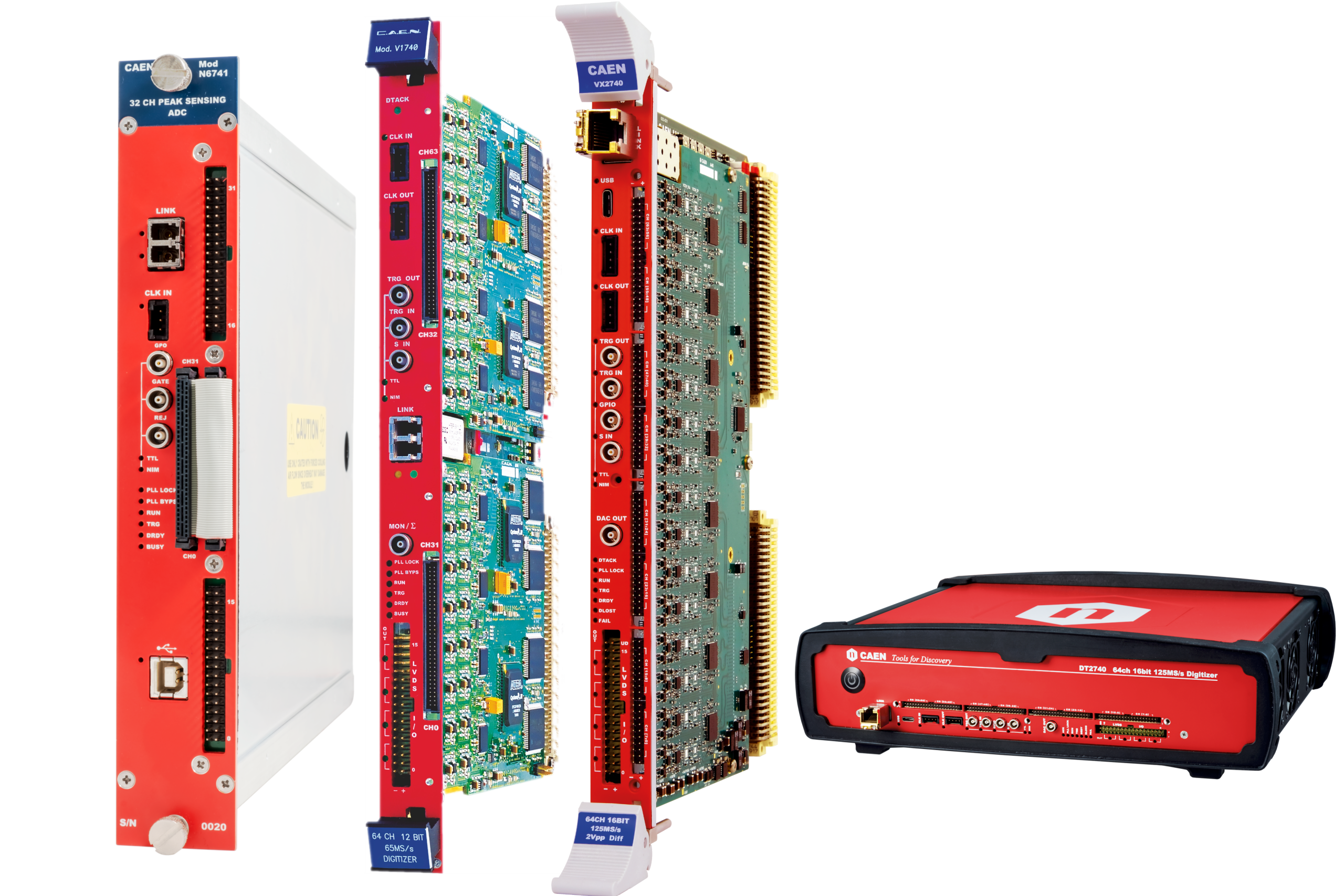
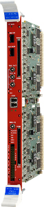
64/32 Ch. 12-bit 62.5 MS/s Digitizer


Digitizers 1.0
740 Digitizer Family
The 740 is a high channel density CAEN Waveform Digitizer family able to perform basic waveform recording and run online advanced algorithms (DPP) of charge integration. Both the elevate number of channels per board (32 for Desktop and NIM form factor, 64 for VME) and the DPP algorithm make the board a digital replacement of a traditional QDC. Data is read by a Flash ADC, 12-bit resolution and 62.5 MS/s sampling rate, which is well suited for mid-slow signals as the ones coming from inorganic scintillators coupled to PMTs, gaseous detectors and others. Sampling rate can be further reduced using the decimation feature. The acquisition can be channel independent and externally vetoed/gated. Multiple boards can be synchronized to build up complex systems.
In case of DPP mode, data can be saved in time-stamped list mode to support higher input rates and improving the throughput performances. The acquisition in DPP mode is fully controlled by the CoMPASS software (Coming Soon), which manages the algorithm parameters, builds the plots and saves the relevant energy and time spectra. In case of waveform recording mode, the user can take advantage of the CAENScope and WaveDump software to access and save the waveforms. Libraries and demo software in C and LabView are available for integration and customization of specific acquisition systems.
740 family comes in three form factors: VME (64 input channels), NIM (32 input channels) and Desktop (32 input channels). The communication to and from the board is provided through the following interfaces: USB (Desktop and NIM form factors), VMEbus (VME form factor), and Optical Link (all form factors).
- 12-bit @ 62.5 MS/s
- Analog inputs on ERNI SMC connectors
- VME64/VME64X (64 ch.), NIM (32 ch.) and Desktop (32 ch.) modules
- 2 or 10 Vpp input dynamic range with programmable DC offset adjustment
- Sampling rate decimation factor (software selectable)
- Algorithms for Digital Pulse Processing (DPP)
- VME, USB and Optical Link communication interfaces
- Multi-board synchronization features
- Daisy chain capability
- Demo software tools, Control Software for waveform recording and DPP firmware, C and LabVIEW libraries
64/32 Ch. 12-bit 62.5 MS/s Digitizer Models
DT5740
DT5740D
-
12 bit 62.5 MS/s ADC
-
32 / 16 channels
-
ERNI SMC Dual Row 68pin connector (32 channels)
-
Auxiliary ERNI SMC Dual Row 68pin connector
-
MCX connectors (16 channels by using auxiliary SMC)
-
2 Vpp single ended input range
-
16-bit programmable DC offset adjustment: ±1 V
-
Trigger Time stamps
-
Memory buffer: 192 kS/ch, up to 1024 events
-
FPGA for real-time data processing:
-
Digital Charge to Digital Converter (DPP-QDC)
-
-
Programmable event size and pre-post trigger adjustment
-
Optical Link interface (CAEN proprietary protocol)
-
USB 2.0 compliant interface
-
Firmware upgradeable via USB or Optical Link
-
Caen DPP-QDC demo software (windows only) with C source file for developers
-
External AC-DC Power Supply Adapter (+12 V)
-
Dimensions: 154x50x164 mm3 (WxHxD)
Obsolete
N6740
-
12 bit 62.5 MS/s ADC
-
32 channels (16 channels on LEMO connectors using A746D adapter)
-
ERNI SMC Dual Row 68pin connector (32 channels)
-
2 Vpp single ended input range (10 Vpp also available)
-
16-bit programmable DC offset adjustment: ±1 V (±5 V)
-
Trigger Time stamps
-
Memory buffer: 192 kS/ch, up to 1024 events
-
FPGA for real-time data processing
-
Programmable event size and pre-post trigger adjustment
-
Optical Link interface (CAEN proprietary protocol)
-
USB2.0 interface
-
Firmware upgradeable via USB/Optical Link
-
Libraries, Demos (C and LabView) and Software tools for Windows and Linux
Obsolete
N6740D
-
12 bit 62.5 MS/s ADC
-
32 channels (16 channels on LEMO connectors using A746D adapter)
-
ERNI SMC Dual Row 68 pin connector (32 channels)
-
2 Vpp single ended input range
-
16-bit programmable DC offset adjustment: ±1 V
-
Trigger Time stamps
-
Memory buffer: 192 kS/ch, up to 1024 events
-
FPGA for real-time data processing:
-
Digital Charge to Digital Converter (DPP-QDC)
-
-
Programmable event size and pre-post trigger adjustment
-
Optical Link interface (CAEN proprietary protocol)
-
USB2.0 interface
-
Firmware upgradeable via USB/Optical Link
-
Libraries, Demos (C and LabView) and Software tools for Windows and Linux
V1740
-
12 bit 62.5 MS/s ADC
-
64 channels
-
Two ERNI SMC Dual Row 68pin connectors (32 + 32 channels)
-
2 Vpp single ended input range (10 Vpp also available)
-
16-bit programmable DC offset adjustment: ±1 V (±5 V)
-
Trigger Time stamps
-
Memory buffer: 192 kS/ch or 1.5 MS/ch, up to 1024 events
-
FPGA for real-time data processing
-
Programmable event size and pre-post trigger adjustment
-
Analog Sum/Majority and digital over/under threshold flags for Global Trigger logic
-
Front panel clock In/Out available for multiboard synchronisation (direct feed through or PLL based synthesis)
-
16 programmable LVDS I/Os
-
Optical Link interface (CAEN proprietary protocol)
-
VME64X compliant interface
-
A2818(PCI) / A3818 (PCIe) Controller available for handling up to 8/32 modules Daisy chained via Optical Link
-
Firmware upgradeable via VME/Optical Link
-
Libraries, Demos (C and LabView) and Software tools for Windows and Linux
V1740D
-
12 bit 62.5 MS/s ADC
-
64 channels
-
Two ERNI SMC Dual Row 68pin connectors (32 + 32 channels)
-
2 Vpp single ended input range
-
16-bit programmable DC offset adjustment: ±1 V
-
Trigger Time stamps
-
Memory buffer: 192 kS/ch, up to 1024 events
-
FPGA for real-time data processing:
-
Digital Charge to Digital Converter (DPP-QDC)
-
-
Programmable event size and pre-post trigger adjustment
-
Analog Sum/Majority and digital over/under threshold flags for Global Trigger logic
-
Front panel clock In/Out available for multiboard synchronisation (direct feed through or PLL based synthesis)
-
16 programmable LVDS I/Os
-
Optical Link interface (CAEN proprietary protocol)
-
VME64X compliant interface
-
A2818 (PCI) / A3818 (PCIe) Controller available for handling up to 8/32 modules Daisy chained via Optical Link
-
Firmware upgradeable via VME/Optical Link
-
Libraries, Demos (C and LabView) and Software tools for Windows and Linux
VX1740
-
12 bit 62.5 MS/s ADC
-
64 channels
-
Two ERNI SMC Dual Row 68pin connectors (32 + 32 channels)
-
2 Vpp single ended input range (10 Vpp also available)
-
16-bit programmable DC offset adjustment: ±1 V (±5 V)
-
Trigger Time stamps
-
Memory buffer: 192 kS/ch or 1.5 MS/ch, up to 1024 events
-
FPGA for real-time data processing
-
Programmable event size and pre-post trigger adjustment
-
Analog Sum/Majority and digital over/under threshold flags for Global Trigger logic
-
Front panel clock In/Out available for multiboard synchronisation (direct feed through or PLL based synthesis)
-
16 programmable LVDS I/Os
-
Optical Link interface (CAEN proprietary protocol)
-
VME64X compliant interface
-
A2818(PCI) / A3818 (PCIe) Controller available for handling up to 8/32 modules Daisy chained via Optical Link
-
Firmware upgradeable via VME/Optical Link
-
Libraries, Demos (C and LabView) and Software tools for Windows and Linux
VX1740D
-
12 bit 62.5 MS/s ADC
-
64 channels
-
Two ERNI SMC Dual Row 68pin connectors (32 + 32 channels)
-
2 Vpp single ended input range
-
16-bit programmable DC offset adjustment: ±1
-
Trigger Time stamps
-
Memory buffer: 192 kS/ch, up to 1024 events
-
FPGA for real-time data processing:
-
Digital Charge to Digital Converter (DPP-QDC)
-
-
Programmable event size and pre-post trigger adjustment
-
Analog Sum/Majority and digital over/under threshold flags for Global Trigger logic
-
Front panel clock In/Out available for multiboard synchronisation (direct feed through or PLL based synthesis)
-
16 programmable LVDS I/Os
-
Optical Link interface (CAEN proprietary protocol)
-
VME64X compliant interface
-
A2818(PCI) / A3818 (PCIe) Controller available for handling up to 8/32 modules Daisy chained via Optical Link
-
Firmware upgradeable via VME/Optical Link
-
Libraries, Demos (C and LabView) and Software tools for Windows and Linux
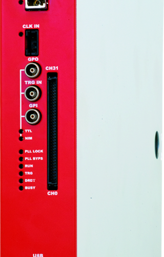
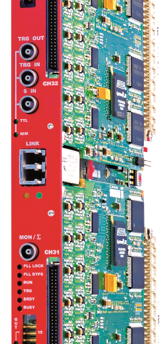
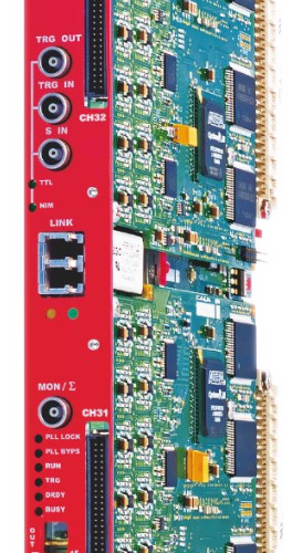
Interfaces & I/O
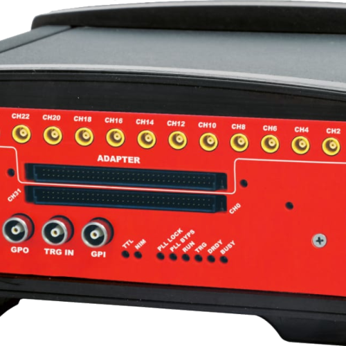
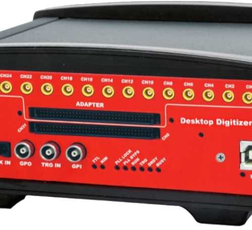
USB
An USB 2.0 link is provided in NIM and Desktop form factors for an easy data readout
VME Digitizer can be controlled via USB using the CAEN V3718 VME-USB2.0 Bridge
Optical Link
An Optical link is provided in any form factor for high performance data readout through CAEN proprietary daisy-chainable CONET communication protocol.
it is possible to connect up to 8/32 ADC modules to a single Optical Link Controller (Mod. A4818/A3818)
Digital I/O
Digital I/Os are provided in VME boards that can be used for individual trigger propagation to external trigger logic. This feature makes VME form factor ideal to scale up the acquisition channels where a global trigger generation is mandatory.
Footer

